Page 1 of 2

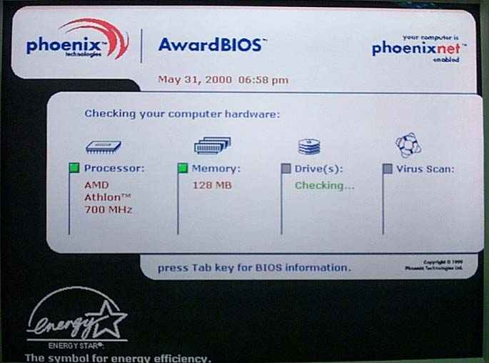
My guide to award BIOS reverse engineering

Posted: Fri Aug 06, 2004 6:55 pm
by maman
I really wish you all to evaluate it guys. Here's the link : http://www.geocities.com/mamanzip/Artic ... guide.html
A snippet of the contents :
---------------------------------------------------------------
Table of Contents
  • 1. Foreword
  • 2. Prerequisite
    • 2.1. PCI BUS
    • 2.2. ISA BUS
  • 3. Some Hardware Peculiarities
    • 3.1. BIOS Chip Addressing
    • 3.2. Obscure Hardware Port
    • 3.3. "Relocatable" Hardware Port
    • 3.4. Expansion ROM Handling
  • 4. Some Software Peculiarities
    • 4.1. Call Instruction Peculiarity
    • 4.2. Retn Instruction Peculiarity
  • 5. Our Tools of Trade
  • 6. Award BIOS File Structure
    • 6.1. The Compressed Components
    • 6.2. The Pure Binary Components
    • 6.3. The Memory Map In The Real System (Mainboard)
  • 7. Disassembling the BIOS
    • 7.1. Bootblock
      • 7.1.1 "Virtual Shutdown" routine
      • 7.1.2 Chipset_Reg_Early_Init routine
      • 7.1.3 Init_Interrupt_n_PwrMgmt routine
      • 7.1.4 Call To "Early Silicon Support" Routine
      • 7.1.5 Bootblock Is Copied And Executed In RAM
      • 7.1.6 Call to bios decompression routine and the jump into decompressed system bios
    • 7.2. System BIOS a.k.a Original.tmp
      • 7.2.1. Entry point from "Bootblock in RAM"
      • 7.2.2. The awardext.rom and Extension BIOS Components (lower 128KB bios-code) Relocation Routine
      • 7.2.3. Call to the POST routine a.k.a "POST jump table execution"
      • 7.2.4. The "segment vector" Routines
      • 7.2.5. "chksum_ROM" Procedure
      • 7.2.6. Original.tmp decompression routine for the "Extension_BIOS components"
  • 8. Closing
----------------------------------------------------------------


I'm looking forward your feedback :D. Thx

Posted: Mon Aug 09, 2004 7:16 pm
by maman
one reader responded with a very interesting information as follows.
written in my article :

There are couples of tricky areas in the BIOS code due to the execution of some of its parts in ROM. I'll present some of my findings below.

call instruction is not available during bios code execution from within BIOS ROM chip. This is due to call instruction uses/manipulate stack while we don't have writeable area in BIOS ROM chip to be used for stack. What I mean by manipulating stack here is the "implicit" push instruction which is executed by the call instruction to "write/save" the return address in the stack. As we know clearly, address pointed to by ss:sp at this point is in ROM, meaning: we can't write into it. If you think, why don't use the RAM altogether ? the DRAM chip is not even available at this point. It hasn't been tested by the BIOS code, thus we haven't know if RAM even exists!


Mark_Larson (a reader of the article) :

Sort of. On current Intel processors there is a feature called Cache As Ram. It allows you to use your cache as if it were RAM before memory is initialized. Cache As Ram is only supported on the latest processors. On older processors in some BIOSes a trick was used to "fake" a stack in the cache. This allowed the BIOS programmer to do CALLs and RETs without memory having been set up. You fake a stack in the cache and then disable the cache. All accesses to the stack come from the cache. The fake stack never gets removed from the cache because the cache is disabled. AMI first did this about 8 years ago.


further explanation from Mark Larson
I'll expand a bit on both parts.

1) Cache As Ram - Intel basically allows you to set the cache to respond to memory acceses from a certain memory range. For instance you could set the memory range 1000h:0 for 8k to be your stack in Cache as Ram. When the processor accesses anything in the 8k range of 1000h:0 it will get the information from the cache. So setting up a stack somewhere is trivial. That allows you to do CALLs and RETs

2) "Faking a stack" -
A) Make sure the L1 is enabled and on and the L2 cache is off.

B) Have 1K ( or however big you want your stack to be), set aside as data in the BIOS ROM chip. Doesn't matter what the 1k of data is, as long as you don't use it for anything else.

C) Read that data in, forcing it to go into the L1 cache ( rep lods).

D) Disable the L1 cache.

E) Now set up the stack through the appropriate commands to point to the data that you just read in.

F) All accesses to the stack now go through the cache, but the data never gets removed from the cache since it's disabled.

G) Having the cache disabled doesn't really mean it's "disabled". What it means is that nothing new can be added to the cache. It still responds to all "hits" with the appropriate data.

As a variation, you can do this with the code in the BIOS ROM as well, and use both the L1 and L2. I only used the L1 to make it easier to illustrate. There is actually an MSR on P3 and earlier processors ( I think it got added in the pentium pro), that lets you directly write to the cache. A lot of 3rd party testing tools use this to test the cache. It works like a memory test. You write a pattern and read it back via this MSR. But you can also use it to load up the data or code you want to use directly into the cache. You can also use that mechanism to create the stack in the cache. However it won't work on P4's. So the above method is more robust, since it works in all cases. AMI if I remember right used the MSR method. Look in Book 3 of any of the processor manuals in the appendix under MSRs ( appendix B). In my P4 book it's under the section "MSRs in the P6 Family Processors". It spans multiple MSRs starting at 88h. Keep in mind that this is no longer on the P4.

Posted: Sat Aug 14, 2004 9:02 pm
by maman
to Moderators. Perhaps this thread can be moved/linked to Collected Wisdom. I think it's worth it for the "potential" reader. Ayway, just an opinion :D. Thx in advance.

Posted: Fri Aug 20, 2004 3:23 am
by Badut
Hi Maman,

Nice article. I haven't had a chance to read it all yet but I will try to do so over the weekend.
I'm just starting to get interested in bios programming.
Hopefully, I'll find the answers to my questions in your article

:D

Posted: Fri Aug 27, 2004 3:48 pm
by maman
in case my website is out of bandwidth, you can download the article at : The CodeBreakers Journal.

Posted: Sat Jul 16, 2005 6:08 am
by maman
just made a minor update to the article again.

CHANGE LOG
-------------------
1. ToC improved for better navigation.
2. BIOS chip addressing improved.
3. Added new sections:
  • "Relocatable" Hardware Port explanation
  • Expansion ROM Handling explanation
4. Better code interpretation :wink:
5. Compressed version of the article can be downloaded as well

translated version

Posted: Tue Oct 18, 2005 10:12 am
by maman
The article has been translated to Russian by my friends at rom.by. Thumbs up and good-work guys. Its accessible at RUKOVODSTVO Pinczakko K ISSLEDOVANIYU PRINTSIPOV RABOTI Award BIOS. Note that this is still the very early version and still a lot things need to be fixed.

Posted: Sun Nov 13, 2005 1:18 pm
by maman
I've added new section for IDA Pro. This section is an introductory material for people who struggle to use IDA Pro. Happy reading and thx goes to people that suggested me to add that section :) .

Posted: Sun Nov 27, 2005 9:05 pm
by Borg Number One
Hi maman.


1.)

In your Guide to Award BIOS reverse engineering, you mention that you are not really sure what the ROSUPD.bin mofule is:

"ROSUPD.bin, seems to be custom Logo display procedure"

Could it be that the module
+ is a "container file" (like an uncompressed zip/rar/... archive)?
+ contains code, fonts and graphics for the graphical award phoenixnet bios P.O.S.T.:

Image
Image Image Image


2.)
Can you check this thread, please?
http://www.wimsbios.com/phpBB2/viewtopic.php?t=7335

Posted: Mon Nov 28, 2005 12:04 am
by Borg Number One
Hi.


Yes, I was/am right...

Download an "Award Modular BIOS" file...:
( e.g. :
http://62.90.2.107/files/boot%20cd/Driv ... 8-bios.exe (Iwill VD133)
http://dl6.mydown.com/home3/bios/kvr1011.exe (Iwill KV200) )
unpack it and open it with CBROM.

If you can see a "ROSUPD.bin" module after displaying the BIOS file's content with CBROM,
then you have a BIOS with a graphical Power On Self Test screen.


I could also successfully extract some graphical stuff:

Image Image Image Image Image
Image

Image Image Image Image Image Image

Image


To get the images from the rosupd.bin:

a)
To find the beginning of a graphic file/data, just look for PG (case sensitive) or look for hex values: "50470001".

b)
Replace each "50470001" with "50470900" to build/get "working" PGX (Phoenix graphics) data.
After this, extract each PG file. (You will see where each PG file ends...)

c)
Run Phoenix BIOS Editor and open any BIOS file with a
"Quiet Boot Logo" module (16 color) and load the PGX files.
In the Phoenix BIOS Editor TEMP directory you will find the currently opened PGX file converted as bitmap.

A Phoenix BIOS with a/some "Splash Screen" modules are useless.
In this case you cannot load PGX files.


You also can download and use Advanced BIOS Logo Reader to open PGX files (Phoenix Graphics):
http://www.kaos.ru/biosgfx/download/abr2-0.16.zip

But the colors may not look "4bit-like" with the Advanced BIOS Logo Reader.


Well, inside the ROSUPD.BIN there is further stuff... :)

E.g. an EBFONT.FON file.
Try fonthack20 [fnthck20] or
ImageJ's ( http://rsb.info.nih.gov/ij/ ) "1bit RAW import feature"
to see the font's content.

The first 1024 bytes of EBFONT.FON do not contain font data.


It would be great, if you could enhance your current
Guide to Award BIOS Reverse Engineering with stuff/documents/file structure of the ROSUPD.BIN file.

Furthermore, it would be great, if you would disassemble the binary stuff / "modules" in the ROSUPD.BIN file.


PS:
The Iwill VD133 BIOS Logo:
Image

is nice. ;)

Posted: Mon Nov 28, 2005 12:57 am
by Borg Number One
Hi.


Here is another interesting bios file with the graphical POST and some more PGX logos:
http://bj.driverchina.com/bios/65me-t22.bin

Posted: Tue Nov 29, 2005 10:21 am
by sunbirds
HI BORG:

there some codes in rosupd.bin

Code: Select all

:0001.16C4 6660                   pushad
:0001.16C6 668B7606               mov esi, [bp+06] ;esi---->PG
:0001.16CA 67813E5047             cmp word ptr [esi], 4750   ;is PG ?
:0001.16CF 0F858E00               jne 1761 ;NO jmp to 1761
:0001.16D3 67660FB74604           movzx eax, word ptr [esi+04] ;eax=0A
:0001.16D9 6603F0                 add esi, eax                ;esi=esi+0A
:0001.16DC 678B06                 mov ax, word ptr [esi]  ;ax=pic width value
:0001.16DF C1E803                 shr ax, 03  ;ax=ax/8
:0001.16E2 2EA37005               mov word ptr cs:[0570], ax
:0001.16E6 678B4602              mov ax, word ptr [esi+02]  ;ax= pic highth value
:0001.16EA 2EA37205               mov word ptr cs:[0572], ax
:0001.16EE 6683C608               add esi, 00000008  ;  esi-->pic content for display
:0001.16F2 8B5E02                 mov bx, [bp+02]
:0001.16F5 8B4604                 mov ax, [bp+04]
:0001.16F8 B95000                 mov cx, 0050 ;cx=50h=80d
:0001.16FB F7E1                   mul cx  ;cx=1900h=6400d
:0001.16FD C1EB03                 shr bx, 03 ;bx=bx/8
:0001.1700 03C3                   add ax, bx
:0001.1702 660FB7F8               movzx edi, word ptr ax
:0001.1706 662E893E6805           mov cs:[0568], edi
:0001.170C BAC403                 mov dx, 03C4 ; 03C4 port : VGA	sequencer register index
:0001.170F B002                   mov al, 02   ;map mask register 
:0001.1711 EE                     out dx, al ; write 03C4 port
:0001.1712 EB00                   jmp 1714

* Referenced by a (U)nconditional or (C)onditional Jump at Address:
|:0001.1712(U)
|
:0001.1714 42                     inc dx  ; dx=dx+1
:0001.1715 EC                     in al, dx ;read port 03c5 :sequencer register data
:0001.1716 2EA26705               mov byte ptr cs:[0567], al
:0001.171A B80201                 mov ax, 0102
:0001.171D 33DB                   xor bx, bx
:0001.171F FC                     cld

* Referenced by a (U)nconditional or (C)onditional Jump at Address:
|:0001.1754(C)
|
:0001.1720 BAC403                 mov dx, 03C4
:0001.1723 EF                     out dx, ax
:0001.1724 662E8B3E6805           mov edi, cs:[0568]
:0001.172A 2E8B0E7205             mov cx, cs:[0572]
:0001.172F 51                     push cx
:0001.1730 662E0FB70E7005         movzx ecx, word ptr cs:[0570]
:0001.1737 6657                   push edi
:0001.1739 6681C700000A00         add edi, 00000000
:0001.1740 F3                     repz
:0001.1741 67A4                   movsb
:0001.1743 665F                   pop edi
:0001.1745 6683C750               add edi, 00000050
:0001.1749 59                     pop cx
:0001.174A E2E3                   loop 172F
:0001.174C B001                   mov al, 01
:0001.174E D1E0                   shl ax, 01
:0001.1750 43                     inc bx
:0001.1751 83FB04                 cmp bx, 0004
:0001.1754 72CA                   jb 1720
:0001.1756 BAC403                 mov dx, 03C4
:0001.1759 2E8A266705             mov ah, cs:[0567]
:0001.175E B002                   mov al, 02
:0001.1760 EF                     out dx, ax

* Referenced by a (U)nconditional or (C)onditional Jump at Address:
|:0001.16CF(C)
|
:0001.1761 6661                   popad
:0001.1763 C3                     ret
port reference:
http://oopweb.com/Assembly/Documents/In ... me/PORTS.B

Posted: Wed Nov 30, 2005 10:05 am
by Borg Number One
Hi.


Thanks for the disassembled code.

The idea would also solve the main problem in this thread:
http://www.wimsbios.com/phpBB2/viewtopic.php?t=7335

"BIOS Logo displaying code - How to detect?"


I just have to unpack the Award BIOS modules and look for: "AWBM" inside the system BIOS module. ;)

If there are "AWBM" strings, then the BIOS can display a small/fullscreen logo. ;)

Posted: Fri Dec 02, 2005 2:43 pm
by maman
Hi Borg, I will incorporate it in the next update of the article. It seems to be it is the current de-facto article on BIOS code analysis :lol: . But, it will take sometime for that.

Thx for your info, I really appreciate it :wink:

NIC EEPROMS - how much $$$ ?

Posted: Sat Dec 17, 2005 6:30 am
by franka2
maman wrote:It seems to be the current de-facto article on BIOS code analysis :lol: .
this seems to hold true ... :D almost like in good old days I read my book "spectrum ROM disassembly"...

some guys might consider to switch to some current mobo with award BIOS (possibly elitegroup featuring top-hat-flash-failproof-eproming) to offset their research activities in this field ...

whats needed now is info which 128KByte eprom fits into those cheapo rtl8139 NIC sockets subsequently to be copied into AMD64 adress space as MENUET64 execute-from-store assembler operating system... :wink:

like this:
The 8139 is probably the most cloned NIC in the world, RTL claims 70% market share

The design of the ethernet controller chip accomodates ROMs up to 128kB which require a 32 pin socket. Some OEMs however use a 28 pin socket because that can hold a 27C512 which can hold up to 64kB of code, more than enough for most cases.

Also recent versions of the controller have the capability of programming EEPROMs in situ. EEPROMs also require a 32 pin socket. But this programming capability isn't always implemented by OEMs because it requires extra circuitry external to the controller and therefore extra cost (a significant fraction of the $5 price).

you have a 28 pin socket: Therefore you need a 27C series EPROM. And an external EPROM programmer (200 €). If you had a 32 pin socket, the 27C010 would also be feasible in addition to the 27C256 and 27C512. The 28 pin ROMs then sit in the socket with the bottom edge aligned (2 empty rows on top, the notch end).